
PCB Printing for OEM Manufacturers: Quality Solutions for Your Projects
When I think about PCB printing, the first thing that comes to mind is the precision and quality I need as a B2B purchaser. Working with OEMs and manufacturers, I rely on exceptional PCB printing solutions that cater to diverse project requirements. With the right partner, I can ensure that the designs are not only accurate but also durable and reliable. Our printing technology stands out in the market, allowing me to get prototypes and mass production runs quickly and efficiently. I appreciate the ability to customize specifications to align with my specific needs, whether I'm looking for single or multilayer boards. And with an experienced team behind the scenes, I feel confident that every order meets industry standards. So, if you're like me and demand the best in PCB printing, let's connect and discuss how we can improve your projects together. Quality materials and exceptional service are just a step away!
Pcb Printing Sets the Industry Standard From Concept to Delivery
In the fast-paced world of electronics, the quality and efficiency of printed circuit boards (PCBs) are crucial to the success of any product. From initial concept to final delivery, the standards set by modern PCB printing processes are reshaping industries globally. By leveraging advanced technologies and innovative methodologies, manufacturers are not only optimizing production timelines but also ensuring that the PCBs meet rigorous quality standards. This commitment to excellence enhances the reliability and performance of electronic devices across various applications. As global demand for high-quality electronic components continues to rise, the importance of seamless collaboration between manufacturers and procurement professionals cannot be overstated. By establishing robust communication channels and understanding the unique requirements of different markets, procurement specialists can ensure that their sourcing strategies align perfectly with manufacturing capabilities. This synergy ultimately leads to better product outcomes and enhanced customer satisfaction, proving that a meticulous approach to PCB production can indeed set a new industry standard. Moreover, sustainability and environmental responsibility are becoming integral to PCB production strategies. Innovative practices are being adopted to minimize waste and energy consumption, reflecting a growing commitment to eco-friendly manufacturing. By choosing partners who prioritize these values, global buyers can not only secure high-quality PCBs but also contribute to a more sustainable future for the electronics industry. Embracing these advancements will drive competitive advantage in the marketplace, fostering long-term growth and innovation for all stakeholders involved.
Pcb Printing Sets the Industry Standard From Concept to Delivery
| Parameter | Value | Description |
|---|---|---|
| Maximum Layer Count | 32 Layers | The maximum number of layers a PCB can have for complex designs. |
| Minimum Trace Width | 4 mils | The smallest width of a conductive trace that can be reliably produced. |
| Minimum Hole Size | 0.2 mm | The smallest diameter of a hole that can be drilled in the PCB. |
| Material Types | FR-4, Rogers, Aluminum | Common materials used for PCBs based on application requirements. |
| Lead Time | 3-5 Days | Typical time taken from order placement to delivery for standard PCBs. |
| Testing Options | Electrical Test, Functional Test | Various testing methods to ensure PCB functionality and reliability. |
| RoHS Compliance | Yes | Indicates compliance with Restriction of Hazardous Substances standards. |
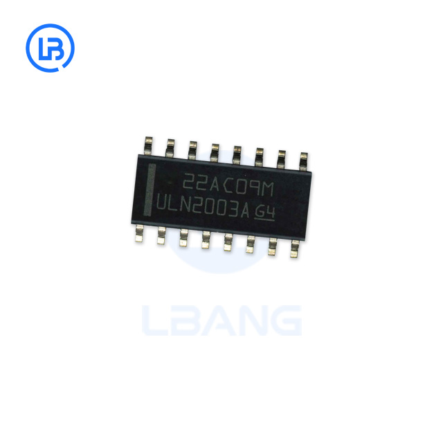
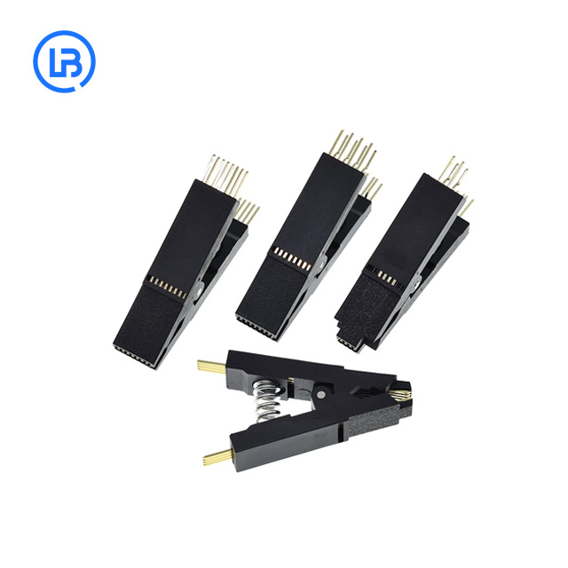
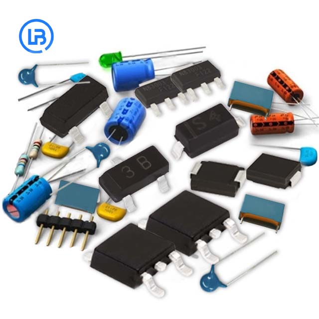
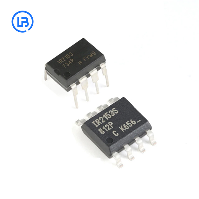
Related Products
Pcb Printing Dominates Factory-Direct Excellence
Top Selling Products
- Related Blog
- Reviews

-

Phone
-

E-mail
-

Whatsapp
WhatsApp
-

Top


